Question 1:
easy
What is the current through an ideal PN-junction diode shown in figure below :
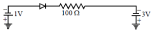
i = 2/100 = 20 mA
What is the current through an ideal PN-junction diode shown in figure below :
i = 2/100 = 20 mA
A reverse biased diode is :
In Reverse bias mode potential of p-type is less than that of n-type semiconductor
A zener diode, having breakdown voltage equal to 15 V, is used in a voltage regulator circuit shown in figure. The current through the zener diode is:
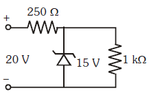
Voltage across 250 ohm resistor= 5 volt
Current through 250 ohm resistor= 5/250 = 20 mA
Current through 1000 ohm resistor = 15/1000 = 15mA
Current through Zener Diode = 20 mA -15 mA = 5 mA
In the following circuit of PN junction diodes D1, D2, D3 are ideal then i is :
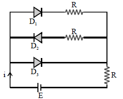
Diode D3 is forward biased so it will short circuit both diodes D1 and D2. So, equivalent resistance of circuit becomes R. Hence,
i= E/R
If in a p-n junction, a square input signal of 10 V is applied as shown, then the output across RL will be :
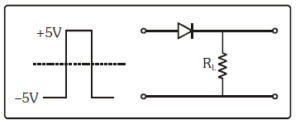
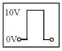
Diode conducts in forward biased case and stops conduction in reverse biased mode.
The breakdown in a reverse biased p–n junction diode is more likely to occur due to

(a) large velocity of the minority charge carriers if the doping concentration is small
(b) large velocity of the minority charge carriers if the doping concentration is large
(c) strong electric field in a depletion region if the doping concentration is small
(d) strong electric field in the depletion region if the doping concentration is large.
The breakdown in a reverse biased p–n junction diode is more likely to occur due to
a. Avalanche Breakdown - large velocity of the minority charge carriers if the doping concentration is small
b. Zener Breakdown - strong electric field in the depletion region if the doping concentration is large
In the following figure, the diodes which are forward biased, are :
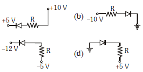
For Forward biasing of PN Junction diode potential of P side should be greater than potential of N-side semiconductor
Which of the following circuits provides full-wave rectification of an ac input :
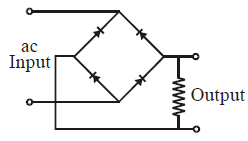
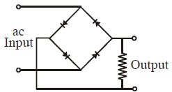
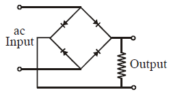
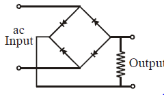
Theoretical question based on bridge rectifier.
A sinusoidal voltage of peak value 200 volt is connected to a diode and resistor R in the
circuit shown so that half-wave rectification occurs. If the forward resistance of the diode
is negligible compared to R, the r.m.s. voltage across R is approximately :
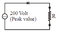
RMS voltage for half wave rectifier is Vmax/2 = 100 Volt
A p–n photodiode is made of a material with a band gap of 2.0 eV. The minimum frequency of the radiation that can be absorbed by the material is nearly :
Energy of EM wave E = hυ
⇒ 2 eV = 6.626 × 10^-34×υ
⇒ \[v= 5\times 10_{14} Hz\]