Question 1:
easy
What is the current through an ideal PN-junction diode shown in figure below :
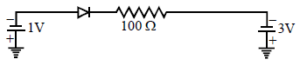
i = 2/100 = 20 mA
What is the current through an ideal PN-junction diode shown in figure below :
i = 2/100 = 20 mA
A reverse biased diode is :
In Reverse bias mode potential of p-type is less than that of n-type semiconductor
In the following figure, the diodes which are forward biased, are :
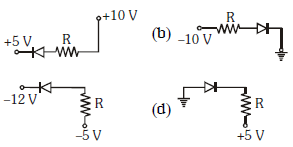
For Forward biasing of PN Junction diode potential of P side should be greater than potential of N-side semiconductor
A p–n photodiode is made of a material with a band gap of 2.0 eV. The minimum frequency of the radiation that can be absorbed by the material is nearly :
Energy of EM wave E = hυ
⇒ 2 eV = 6.626 × 10^-34×υ
⇒ \[v= 5\times 10_{14} Hz\]
When a PN junction diode is reverse biased :
Factual Question: When a PN junction diode is reverse biased potential barrier of depletion increases. Thus Electrons and holes move away from the junction depletion region.
The dominant mechanism for motion of charge carriers in forward and reverse biased silicon P-N junction are :
Theory: In forward biased mode diffusion current is more than drift current. Where as in reverse biased mode diffusion current decreased and become less than drift current.
In the given circuit
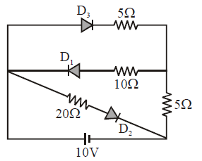
The current through the battery is :
Diode D2 and D3 are forward biased. Where as Diode D1 is reversed biased. No current will flow through D1.
Equivalent Resistance= 20/3 ohm
Current = Voltage / Resistance = 10/ (20/3) = 1.5 Ampere
Phodiode, zenerdiode and solar cell is used in:
A Photodiode and Zener Diode operate in Reverse Bias, while a Solar Cell operates in an Unbiased condition (zero external voltage).
Which of the following statement is not correct when a junction diode is in forward bias :
In forward bias, the applied field opposes the barrier field, pushing major carriers (electrons on n-side and holes on p-side) towards the junction, thereby decreasing the depletion width. Thus, statement (4) is incorrect.
The approximate ratio of resistances in the forward and reverse bias of the PN-junction diode is :
Forward resistance of a diode is very small (\(approx 10\Omega\)), while its reverse resistance is extremely high (\(approx 10^5 \Omega\)). The ratio \(R_f / R_r\) is of the order of \(10^{-4}\), which corresponds to \(1 : 10^4\).