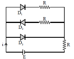
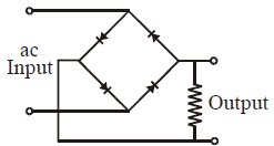
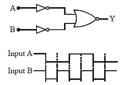
Semiconductor Physics - NEET Physics Questions
← All Chapters

Semiconductor Physics

Question 1: moderate

Intrinsic germanium and silicon at absolute zero temperature behave like :

1. Superconductor
2. Good semiconductor
3. Ideal insulator
4. Conductor
View Answer

At absolute zero temperature (0 K), intrinsic germanium and silicon behave like insulators due to the following reasons:

  1. No Free Charge Carriers: At absolute zero, all the electrons in the material occupy the lowest energy states, and there are no thermally excited electrons available to conduct electricity. This means there are no free charge carriers (electrons or holes).
  2. Wide Band Gap: Both germanium and silicon have a band gap (about 0.66 eV for germanium and 1.1 eV for silicon). At absolute zero, the thermal energy is insufficient to excite electrons across this band gap from the valence band to the conduction band.

As a result, intrinsic germanium and silicon cannot conduct electricity at absolute zero, behaving as insulators.

Question 2: moderate

In the following circuit of PN junction diodes D1, D2, D3 are ideal then i is :

1. E/R
2. E/2R
3. 2E/3R
4. Zero
View Answer

Diode D3 is forward biased so it will short circuit both diodes D1 and D2. So, equivalent resistance of circuit becomes R. Hence,

i= E/R

Question 3: moderate

If in a p-n junction, a square input signal of 10 V is applied as shown, then the output across RL will be :


1.
2.
3.
4.
View Answer

Diode conducts in forward biased case and stops conduction in reverse biased mode.

Question 4: moderate
The breakdown in a reverse biased p–n junction diode is more likely to occur due to

(a) large velocity of the minority charge carriers if the doping concentration is small
(b) large velocity of the minority charge carriers if the doping concentration is large
(c) strong electric field in a depletion region if the doping concentration is small
(d) strong electric field in the depletion region if the doping concentration is large.
1. a, d
2. c only
3. b only
4. b, c
View Answer

The breakdown in a reverse biased p–n junction diode is more likely to occur due to

a. Avalanche Breakdown - large velocity of the minority charge carriers if the doping concentration is small

b. Zener Breakdown -Ā  strong electric field in the depletion region if the doping concentration is large

Question 5: moderate

If A and B are input wave forms for given combination of logic gates then output waveform will be :

1.
2.
3.
4.
View Answer
Question 6: moderate

Find output Y :

1. P + Q
2. \[\overline{P}+P, Q\]
3. \[\overline{P}+\overline{Q}\]
4. None of these
View Answer
Question 7: moderate

If the ratio of the concentration of electrons to that of holes in a semiconductor is 7/5 and the ratio of currents is 7/4 then what is the ratio of their drift velocities :

1. 5/8
2. 4/5
3. 5/4
4. 4/7
View Answer

The ratio of electron to hole currents is given by:

InIp=74\frac{I_n}{I_p} = \frac{7}{4}

The ratio of electron to hole concentrations is:

np=75\frac{n}{p} = \frac{7}{5}

Using the current formula

I=qnvAI = q n v A

, the ratio of drift velocities (

vnvp\frac{v_n}{v_p}

) can be found as:


InIp=nvnpvp

Substitute the given ratios:

74=75ā‹…vnvp\frac{7}{4} = \frac{\frac{7}{5} \cdot v_n}{v_p}

Simplifying:

vnvp=54

Question 8: moderate

Which of the following circuits provides full-wave rectification of an ac input :

1.
2.
3.
4.
View Answer

Theoretical question based on bridge rectifier.Ā 

Question 9: moderate

A sinusoidal voltage of peak value 200 volt is connected to a diode and resistor R in the
circuit shown so that half-wave rectification occurs. If the forward resistance of the diode
is negligible compared to R, the r.m.s. voltage across R is approximately :

1. 200
2. 100
3. 100/√2
4. 283
View Answer

RMS voltage for half wave rectifier is Vmax/2 = 100 Volt

Question 10: moderate

The logic circuit shown below has the input waveforms ‘A’ and ‘B’ as shown. Pick out the correct output waveform.

1.
2.
3.
4.
View Answer