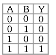
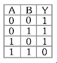
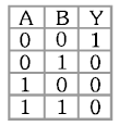
Semiconductor Physics - NEET Physics Questions
← All Chapters

Semiconductor Physics

Question 1: easy

In case of a semiconductor, which of the following statement is wrong :

1. Doping increases conductivity
2. Temperature coefficient of resistance is negative
3. Resisitivity is in between that of a conductor and insulator
4. At absolute zero temperature, it behaves like a conductor
View Answer

The statement "At absolute zero temperature, it behaves like a conductor" is wrong for a semiconductor.

Explanation:

  • At absolute zero (0 K), intrinsic semiconductors (like silicon and germanium) do not have free charge carriers (electrons and holes) because all the electrons occupy the valence band, and there is no thermal energy available to promote them to the conduction band.
  • Therefore, intrinsic semiconductors behave like insulators at absolute zero, not conductors.
Question 2: easy

A conducting wire of Copper and Germanium are cooled from room temperature to temperature 80K, then their resistance will :

1. increase
2. decrease
3. copper's increase and Germanium's decrease
4. copper's decrease and Germanium's increase
View Answer

When a conducting wire of Copper and Germanium is cooled from room temperature to 80K:

  • Copper (metal): Its resistance will decrease because metals have lower resistance at lower temperatures due to reduced electron scattering.
  • Germanium (semiconductor): Its resistance will increase because the number of charge carriers (electrons and holes) decreases at lower temperatures, leading to higher resistance.

Thus, Copper's resistance decreases, while Germanium's resistance increases when cooled to 80K

Question 3: easy

What is the current through an ideal PN-junction diode shown in figure below :

1. Zero
2. 10 mA
3. 20 mA
4. 50 mA
View Answer

i = 2/100 = 20 mA 

Question 4: easy

A reverse biased diode is :

1.
2.
3.
4.
View Answer

In Reverse bias mode potential of p-type is less than that of n-type semiconductor

Question 6: easy

In the following circuit, the output Y for all possible inputs A and B is expressed by the truth table :

1.
2.
3.
4.
View Answer
Question 7: easy

Which statement is correct ?

1. N-type germanium is negatively charged and P-type germanium is positively charged
2. Both N-type and P-type germanium are neutral
3. N-type germanium is positively charged and P-type germanium is negatively charged
4. Both N-type and P-type germanium are negatively charged
View Answer

Both N-type and P-type germanium are electrically neutral because, while they have an imbalance of charge carriers (electrons or holes), the overall number of positive and negative charges remains equal.

- **N-type**: Donor atoms add extra electrons (negatively charged carriers), but the atoms themselves become positively charged ions. This ensures charge neutrality.

- **P-type**: Acceptor atoms create holes (positively charged carriers) by accepting electrons, but the atoms become negatively charged ions. This balances the charge.

In both cases, the total positive and negative charges cancel each other out, keeping the material electrically neutral.

Question 8: easy

Wires P and Q have the same resistance at ordinary (room) temperature. When heated, resistance of P increases and that of Q decreases. We conclude that :

1. P and Q are conductors of different materials
2. P is N-type semiconductor and Q is P-type semiconductor
3. P is semiconductor and Q is conductor
4. P is conductor and Q is semiconductor
View Answer

Resistance of conductor increases with increasing temperature and resistance of semiconductor decreases with increasing temperature.

Question 9: easy

The resistivity of a pure semiconductor is 0.5 Ωm. If the electron and hole mobility be
0.39 m²/V-s and 0.19 m²/V-s respectively then calculate the intrinsic carrier concentration.

1. \[2.16\times 10^{19}/m^{3}\]
2. \[4.32\times 10^{19}/m^{3}\]
3. \[10^{20}/m^{3}\]
4. \[10^{30}/m^{3}\]
View Answer

The resistivity () of a pure (intrinsic) semiconductor is given by the formula:


ρ=1q(ni)(μn+μp)\rho = \frac{1}{q (n_i) (\mu_n + \mu_p)}

Where:


  • ρ=0.5Ωm\rho = 0.5 \, \Omega\text{m}
     

    (resistivity),


  • q=1.6×10¹⁹Cq = 1.6 \times 10^{-19} \, \text{C}
     

    (charge of an electron),


  • nin_i
     

    = intrinsic carrier concentration (to be calculated),


  • μn=0.39m2/V-s\mu_n = 0.39 \, \text{m}^2/\text{V-s}
     

    (electron mobility),


  • μp=0.19m2/V-s\mu_p = 0.19 \, \text{m}^2/\text{V-s}
     

    (hole mobility).

Rearranging the formula to solve for

nin_i

:


ni=1qρ(μn+μp)n_i = \frac{1}{q \rho (\mu_n + \mu_p)}

Substitute the values:


ni=1(1.6×10¹⁹)(0.5)(0.39+0.19)n_i = \frac{1}{(1.6 \times 10^{-19})(0.5)(0.39 + 0.19)}

ni=1(1.6×10¹⁹)(0.5)(0.58)n_i = \frac{1}{(1.6 \times 10^{-19})(0.5)(0.58)}


ni=14.64×1020=2.16×10¹⁹m3


Thus, the intrinsic carrier concentration

nin_i

is

2.16×10¹⁹m32.16 \times 10^{19} \, \text{m}^{-3}


Question 10: easy

In the following figure, the diodes which are forward biased, are :

1. (a), (b) and (d)
2. (c) only
3. (a) and (c)
4. (b) and (d)
View Answer

For Forward biasing of PN Junction diode potential of P side should be greater than potential of N-side semiconductor