Semiconductor Physics - NEET Physics Questions
← All Chapters

Semiconductor Physics

Question 41: easy

The dominant mechanism for motion of charge carriers in forward and reverse biased silicon P-N junction are :

1. Drift in forward bias, diffusion in reverse bias
2. Diffusion in forward bias, drift in reverse bias
3. Diffusion in both forward and reverse bias
4. Drift in both forward and reverse bias
View Answer

Theory: In forward biased mode diffusion current is more than drift current. Where as in reverse biased mode diffusion current decreased and become less than drift current.
Question 42: easy

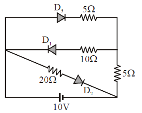
In the given circuit

The current through the battery is :

1. 0.5 A
2. 1 A
3. 1.5 A
4. 2 A
View Answer

Diode D2 and D3 are forward biased. Where as Diode D1 is reversed biased. No current will flow through D1. 

Equivalent Resistance= 20/3 ohm

Current = Voltage / Resistance = 10/ (20/3) = 1.5 Ampere

Question 43: easy

Phodiode, zenerdiode and solar cell is used in:

1. Forward Bias, Reverse Bias, Forward Bias
2. Reverse Bias, Reverse Bias, Unbiased
3. Reverse Bias, UnBias, Reverse Bias
4. Reverse Bias, Reverse Bias, Reverse Bias
View Answer

A Photodiode and Zener Diode operate in Reverse Bias, while a Solar Cell operates in an Unbiased condition (zero external voltage).

  • Photodiode: Works in reverse bias to detect light.
  • Zener Diode: Operates in reverse bias for voltage regulation.
  • Solar Cell: Generates power in an unbiased condition when exposed to light.
Question 44: easy

Which of the following statement is not correct when a junction diode is in forward bias :

1. The width of depletion region decrease
2. Free electrons on n-side will move towards the junction
3. Holes on p-side move towards the junction
4. Electrons on n-side and holes on p-side will move away from junction
View Answer

In forward bias, the applied field opposes the barrier field, pushing major carriers (electrons on n-side and holes on p-side) towards the junction, thereby decreasing the depletion width. Thus, statement (4) is incorrect.

Question 45: easy

The approximate ratio of resistances in the forward and reverse bias of the PN-junction diode is :

1. \(10^2 : 1\)
2. \(10^{-2} : 1\)
3. \(1 : 10^{-4}\)
4. \(1 : 10^4\)
View Answer

Forward resistance of a diode is very small (\(approx 10\Omega\)), while its reverse resistance is extremely high (\(approx 10^5 \Omega\)). The ratio \(R_f / R_r\) is of the order of \(10^{-4}\), which corresponds to \(1 : 10^4\).

Question 46: easy

A p-type extrinsic semiconductor is obtained when Germanium is doped with

1. Arsenic
2. Boron
3. Antimony
4. Phosphorous
View Answer

A p-type semiconductor is created by doping a tetravalent semiconductor (like Ge) with a trivalent impurity such as Boron.

Question 47: easy

Consider the following statements (A) and (B) and identify the correct answer.


(A) A zener diode is connected in reverse bias, when used as a voltage regulator.


(B) The potential barrier of \(p\)-\(n\) junction lies between 0.1 V to 0.3 V.

1. (A) is incorrect but (B) is correct.
2. (A) and (B) both are correct.
3. (A) and (B) both are incorrect.
4. (A) is correct and (B) is incorrect.
View Answer

A Zener diode regulates voltage when reverse-biased in the breakdown region (A is correct). The potential barrier for a Silicon p-n junction is around 0.7 V, which is outside the 0.1 V to 0.3 V range (B is incorrect).

Question 48: easy

The electron concentration in an \(n\)-type semiconductor is the same as hole concentration in a \(p\)-type semiconductor. An external field (electric) is applied across each of them. Compare the currents in them.

1. No current will flow in \(p\)-type, current will only flow in \(n\)-type
2. Current in \(n\)-type = current in \(p\)-type
3. Current in \(p\)-type > current in \(n\)-type
4. Current in \(n\)-type > current in \(p\)-type.
View Answer

The mobility of electrons (\(mu_e\)) is greater than the mobility of holes (\(mu_h\)). Since current is proportional to mobility for the same carrier concentration and electric field, the current in the \(n\)-type semiconductor is greater than that in the \(p\)-type.

Question 49: easy

A silicon (Si) specimen is doped with aluminium (Al). The concentration of acceptor atoms is \(10^{18}\text{ m}^{-3}\). Given that the intrinsic carrier concentration is \(10^{16}\text{ m}^{-3}\), the concentration of electrons in the specimen is

1. 10^{14} m^{-3}
2. 10^{16} m^{-3}
3. 10^{18} m^{-3}
4. 10^{12} m^{-3}
View Answer

Formula: \(n_e n_h = n_i^2\). Since the semiconductor is heavily p-doped, \(n_h approx N_a = 10^{18}\text{ m}^{-3}\). Therefore, \(n_e = frac{n_i^2}{n_h} = frac{(10^{16})^2}{10^{18}} = 10^{14}\text{ m}^{-3}\).

Question 50: easy

Given below are two statements: one is labelled as Assertion (A) and the other is labelled as Reason (R).


Assertion (A): A digital circuit that follows logical relationship between the input and output voltages are generally known as logic gates.


Reason (R): NOR and NAND gates are not considered as universal gates.


In the light of above statements, choose the correct answer from the options given below.

1. Both (A) and (R) are true and (R) is the correct explanation of (A)
2. Both (A) and (R) are true but (R) is not the correct explanation of (A)
3. (A) is true but (R) is false
4. Both (A) and (R) are false
View Answer

Assertion is true because logic gates process signals based on logical relationships. Reason is false because NAND and NOR gates can implement any Boolean function, meaning they are universal gates.