Question 31:
moderate
Figure gives a system of logic gates. From the study of truth table it can be found that to produce a high output (1) at R, we must have :
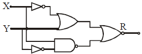
Figure gives a system of logic gates. From the study of truth table it can be found that to produce a high output (1) at R, we must have :
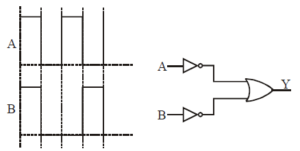
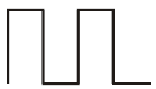
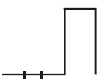
In a given circuit as shown the two input wave form A and B are applied simultaneously. The
resultant waveform Y is :
Which one of the following statement is FALSE :
Majority charge carrier in N-type semiconductor is electrons and in P-type semiconductor is holes
Representation of N-type semiconductor is :
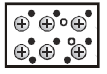
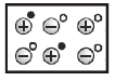
In N type semiconductor number of electrons is more than number of holes
The resistivity of a pure semiconductor is 0.5 Ωm. If the electron and hole mobility be 0.39 m²/V-s and 0.19 m²/V-s respectively then calculate the intrinsic carrier concentration.
A Ge specimen is doped with Al. The concentration of acceptor atoms is \[\sim 10^{21} atom/m^{3}\]. Given that the intrinsic concentration of electron hole pairs is \[\sim 10^{19}/m^{3}\], the concentration of electrons in the specimen is :
According to mass action law
\[ n_{e}\times n_{h}= n_{i}^{2} \]
\[ n_{h}=10^{21} ; n_{i}= 10^{19}; n_{e}=n_{i}^{2}/n_{h} = n_{e}= 10^{38}/10^{21}= 10^{17} \]
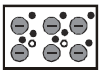
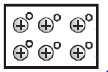
Intrinsic semiconductor is electrically neutral. Extrinsic semiconductor having large number of current carriers would be :
An extrinsic semiconductor with a large number of current carriers is still electrically neutral overall because the total number of positive and negative charges remains balanced.
The contribution in the total current flowing through a semiconductor due to electrons and holes are 3/4 and 1/4 respectively. If the drift velocity of electrons is 5/2 times that of holes at this temperature, then the ratio of concentration of electrons and holes is :
Current i = neAv
\[ \frac{I_{1}}{I_{2}}= \frac{n_{1}}{n_{2}} * \frac{v_{d1}}{v_{d2}} \]
\[ \frac{3}{1}= \frac{n_{1}}{n_{2}} * \frac{5}{2} \]
\[ \frac{n_{1}}{n_{2}} = \frac{6}{5} \]
When a PN junction diode is reverse biased :
Factual Question: When a PN junction diode is reverse biased potential barrier of depletion increases. Thus Electrons and holes move away from the junction depletion region.
Two PN-junctions can be connected in series by three different methods as shown in the figure. If the potential difference in the junctions is the same, then the correct connections will be :
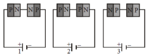
In circuit 1. First Diode is forward biased and second diode is reverse biased. So, potential across 1st diode is less than 2nd diode.
In circuit 2: Both the diodes are forward biased so potential difference across them is equal
In circuit 3: Both the diodes are reverse biased so potential difference across them is equal to V/2.