Question 1:
easyWhat is the current through an ideal PN-junction diode shown in figure below :
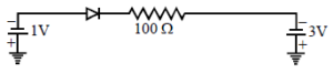
i = 2/100 = 20 mA
Question 1:
easyWhat is the current through an ideal PN-junction diode shown in figure below :
i = 2/100 = 20 mA
Question 2:
easyA reverse biased diode is :
In Reverse bias mode potential of p-type is less than that of n-type semiconductor
Question 3:
easyIn the following figure, the diodes which are forward biased, are :
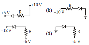
For Forward biasing of PN Junction diode potential of P side should be greater than potential of N-side semiconductor
Question 4:
easyA p–n photodiode is made of a material with a band gap of 2.0 eV. The minimum frequency of the radiation that can be absorbed by the material is nearly :
Energy of EM wave E = hυ
⇒ 2 eV = 6.626 × 10^-34×υ
⇒ \[v= 5\times 10_{14} Hz\]
Question 5:
easyWhen a PN junction diode is reverse biased :
Factual Question: When a PN junction diode is reverse biased potential barrier of depletion increases. Thus Electrons and holes move away from the junction depletion region.
Question 6:
easyThe dominant mechanism for motion of charge carriers in forward and reverse biased silicon P-N junction are :
Theory: In forward biased mode diffusion current is more than drift current. Where as in reverse biased mode diffusion current decreased and become less than drift current.
Question 7:
easyIn the given circuit
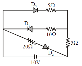
The current through the battery is :
Diode D2 and D3 are forward biased. Where as Diode D1 is reversed biased. No current will flow through D1.
Equivalent Resistance= 20/3 ohm
Current = Voltage / Resistance = 10/ (20/3) = 1.5 Ampere
Question 8:
easyPhodiode, zenerdiode and solar cell is used in:
A Photodiode and Zener Diode operate in Reverse Bias, while a Solar Cell operates in an Unbiased condition (zero external voltage).
Question 9:
easyWhich of the following statement is not correct when a junction diode is in forward bias :
In forward bias, the applied field opposes the barrier field, pushing major carriers (electrons on n-side and holes on p-side) towards the junction, thereby decreasing the depletion width. Thus, statement (4) is incorrect.
Question 10:
easyThe approximate ratio of resistances in the forward and reverse bias of the PN-junction diode is :
Forward resistance of a diode is very small (\(approx 10\Omega\)), while its reverse resistance is extremely high (\(approx 10^5 \Omega\)). The ratio \(R_f / R_r\) is of the order of \(10^{-4}\), which corresponds to \(1 : 10^4\).